______ Limits the dv/dt across the switching device during ______
| ______ Limits the dv/dt across the switching device during ______.
A. Snubber, turnoff of the device
B. Inductor, turnoff of the device
C. Inductor, normal running conditions
D. Snubber, normal running conditions
Please scroll down to see the correct answer and solution guide.
Right Answer is: A
SOLUTION
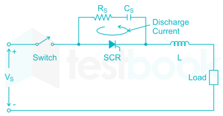
dv/dt protection:
- When the SCR is forward biased, junctions J1 and J3 are forward biased and junction J2 is reverse biased. This reverse biased junction J2 exhibits the characteristics of a capacitor.
- If the rate of forward voltage applied is very high across the SCR, charging current flows through the junction J2 is high. This current is enough to turn ON the SCR even without any gate signal.
- This is called as dv/dt triggering of the SCR. This can be reduced by using RC snubber network across the SCR.
- A snubber circuit consists of a series combination of resistance Rs and capacitance Cs in parallel with the thyristor.
- False turn – ON of an SCR by large dv/dt, even without application of gate signal can be prevented by using a snubber circuit.
- Snubber limits the dv/dt across the switching device during turnoff of the device .
